Superior Diamond
Properties for
Thermal Management
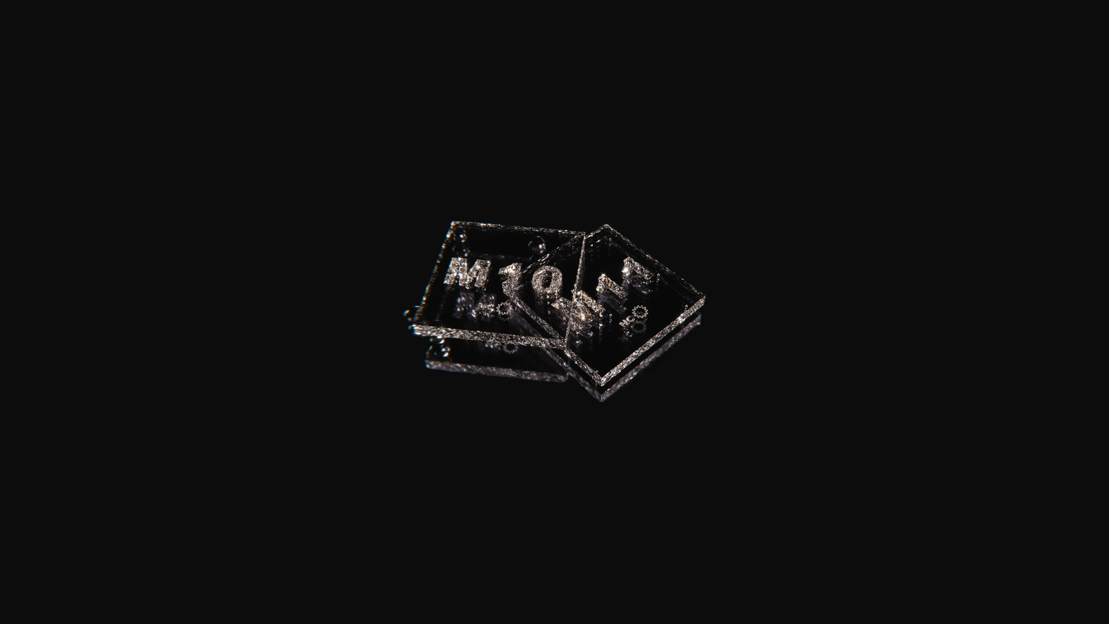
M10 and M11 single crystal diamonds deliver industry-leading thermal conductivity and precision engineering for high-performance devices and lasers.
How Northern Carbon Improves Heat Management
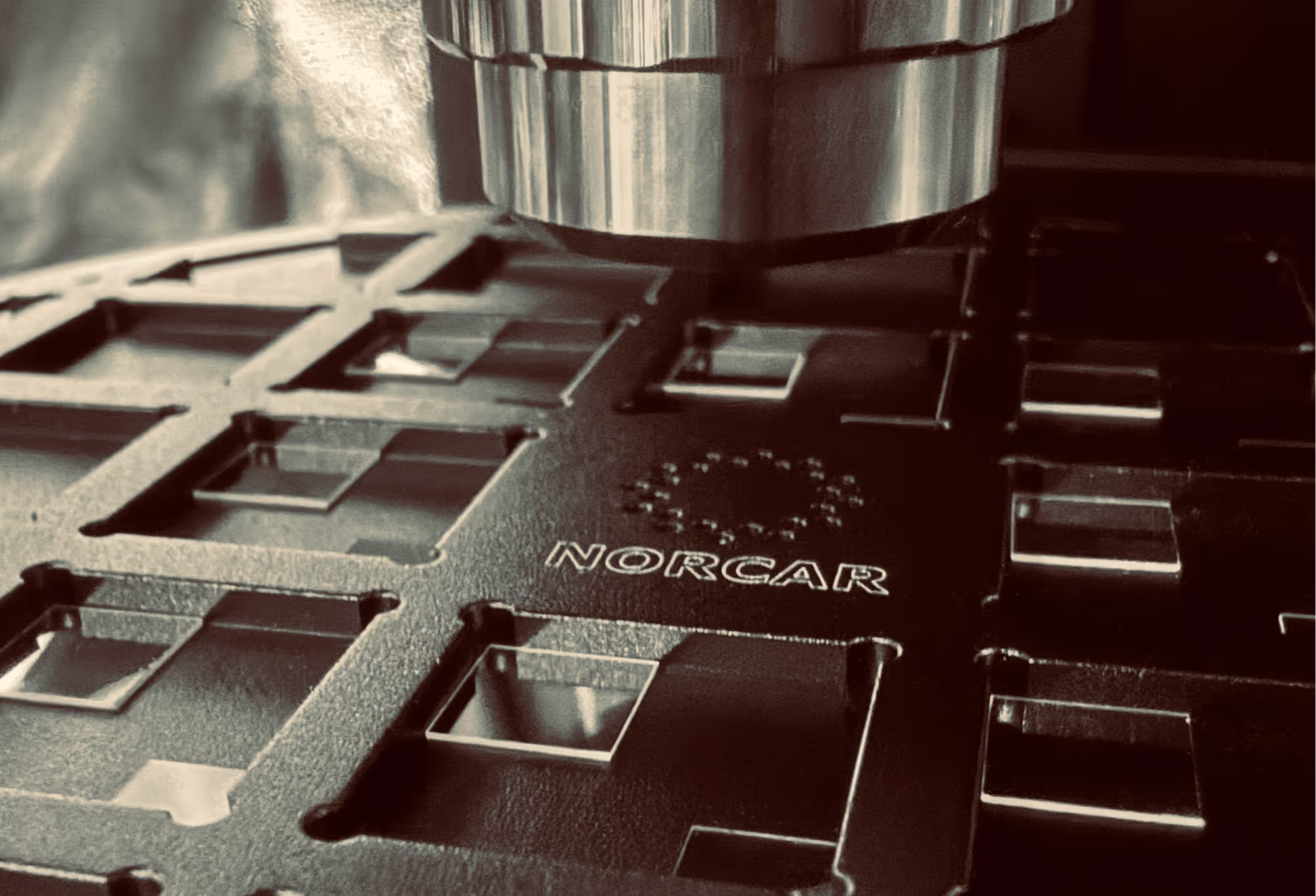
M10 is engineered to extract and dissipate heat from the most demanding electronic devices. By rapidly spreading heat isotropically, M10 minimizes hotspots, enhances reliability, and enables higher sustained performance.
Built with Precision, Ready for Deployment
M10 and M11 are engineered through microwave plasma CVD growth, followed by laser cutting and chemo-mechanical polishing to nanometer or sub-nanometer precision.
01Integration & Deployment Highlights
Integration & Deployment Highlights
• Designed for integration into existing optoelectronic packages and attachment to heat sinks.
• Metallization layer thickness is tailored to the application:
- 0.5–1 µm for CPU/GPU chips
- 3–5 µm for laser diodes
• Soldered attachment via standard Au/Sn preforms for reliable thermal and electrical contact.
• Supports large-scale semiconductor assembly.
02APPLICATIONS
Applications
• CPUs, GPUs, and AI accelerators
• Power amplifiers and laser diodes
• Advanced manufacturing and optical devices
Unlock Maximum
Performance with
M10 & M11
Discover why our single crystal diamonds can prevent hotspots, improve thermal efficiency, and extend the lifespan of your most critical chips, lasers, and high-performance electronics.