M11: Next-Generation Diamond for Extreme Device Performance
M11 pushes the limits of heat management and precision integration, engineered for the highest-power AI accelerators, laser systems, and advanced optical devices.
.webp)
Impact & Performance
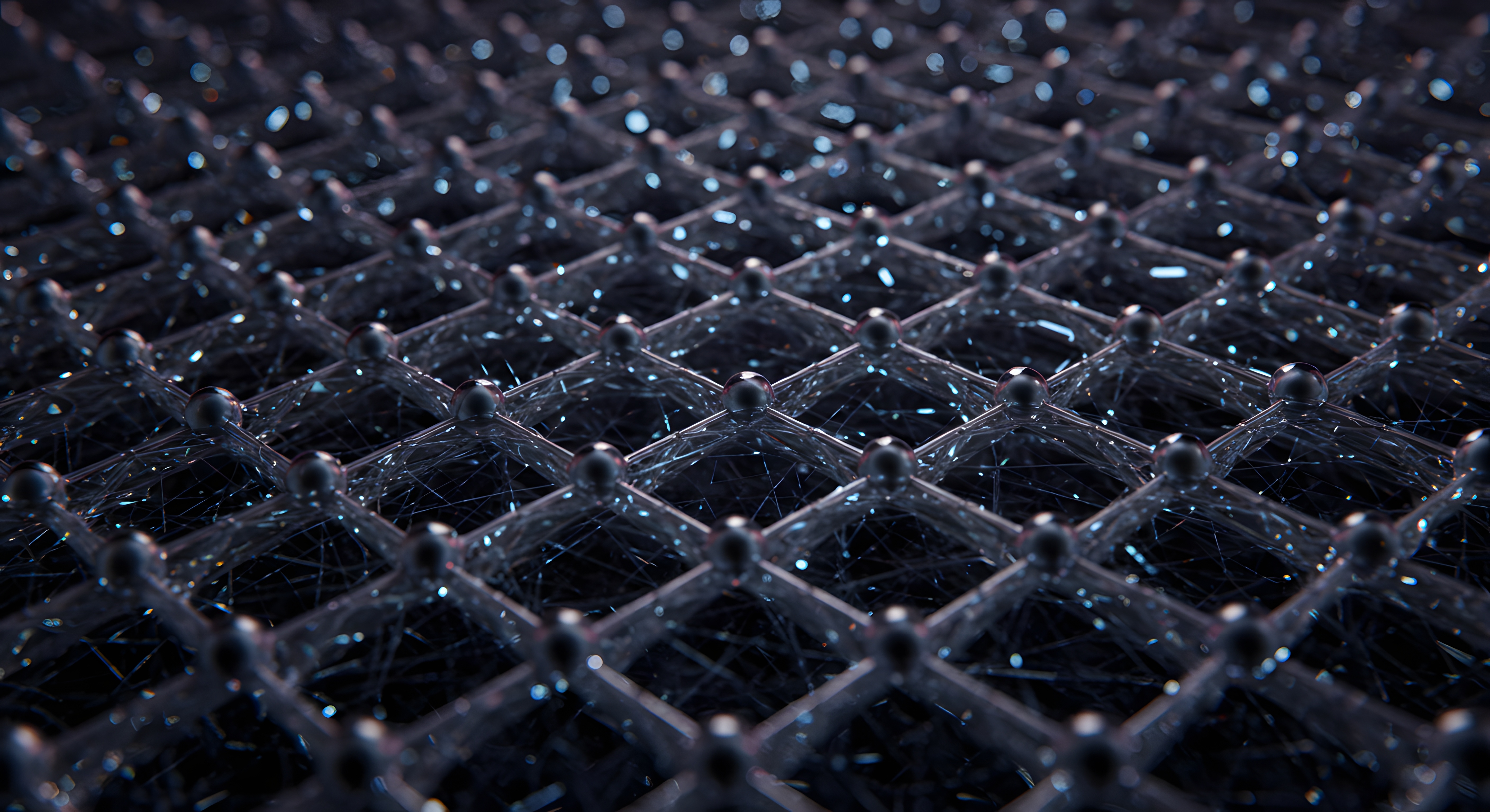
M11 is designed for the most demanding wide bandgap device, for special thermal and optical applications, delivering consistent lateral heat transfer and ultra-stable performance under extreme conditions.
01Targeting Extreme Hotspots
Targeting Extreme Hotspots
M11 spreads concentrated heat as well as M10, maintaining efficiency and reliability in high-density, high-power systems for next generation devices.
.webp)
02Maximize Device Reliability
Maximize Device Reliability
Lowering junction temperature by 10–15°C extends lifespan and ensures sustained performance in mission-critical applications.
.webp)
03Atomic-Level Control
Atomic-Level Control
Manufactured to sub-nanometer tolerances with optional metallization layers, M11 supports devices with unique current, RF, and photonic requirements.
.webp)
Technical Overview
M11 is built for the most demanding thermal and integration environments, combining ultra-high conductivity with atomic-level surface control. It is suited for advanced devices where thermal stability, reliability, and specialized packaging requirements are essential.
Lapped ~ 150-250nm
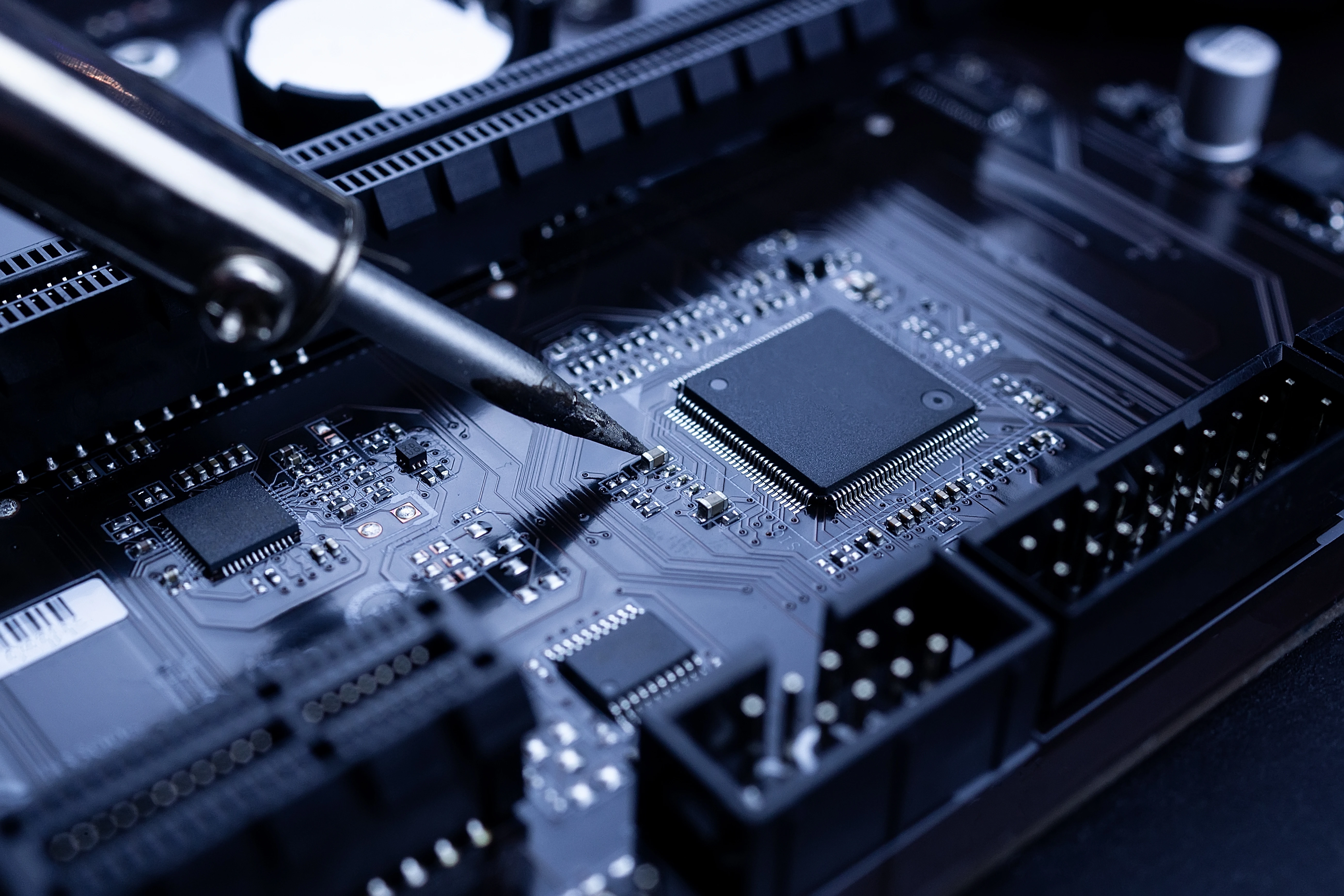
Manufacturing & Integration
M11 combines advanced growth, precision engineering, and tailored integration to support cutting-edge applications.
Atomic-Level Precision
Custom Metallization

Solder & Bonding Flexibility
Rigorous QA & Metrology

Tailored Integration
.webp)
Integrate M11 Into Your Advanced Systems
M11 enables next-level thermal and optical management for high-power and high-density devices. Deploy M11 to maximize reliability, efficiency, and lifespan in the most demanding electronic and photonic systems.